Cover Story
CEOCFO
Interview
Index &
Quotes
CEOCFO
Current Issue
Future
Features
Monthly
Analyst
Industry
Review
Analyst
Interviews
and Reports
Corporate
Financials
Archived
CEOCFO
Interviews
About
CEOCFO
interviews.com
Contact
& Ordering |
"To print this page go to file and left
click on print"
Introduction of new products and
expansion of its customer base has CyberOptics well positioned for the recovery of the
electronic assembly and semiconductor capital equipment markets

Technology
Scientific & Technical Instruments
NASD: CYBE
Cyber Optics Corp.
5900 Golden Hills Drive
Minneapolis, MN 55416
Phone: 763-542-5000
Steven Quist
Chief Executive Officer
Interview conducted by:
Walter Banks
Co-Publisher
CEOCFOinterviews.com
August 2002
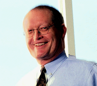
Bio of CEO,
Steven M. Quist
CyberOptics Corporation
5900 Golden Hills Drive, Minneapolis, MN 55416
Steven M. Quist joined CyberOptics Corporation (NasdaqNMS: CYBE) March 1998 as
president and CEO. Mr. Quist had served on
the Company's board of directors since 1991. Quist previously was president of Rosemount
Inc. of Eden Prairie, MN, a leading multinational manufacturer of high-performance
instrumentation for the processing industries. Rosemount is a subsidiary of Emerson
Electric Co., St. Louis, MO (NYSE: EMR).
In previous
assignments with Rosemount, Quist was responsible for advanced technology developments
including a state-of-the-art MEMS technology facility, Emerson Electric’s first
technology center of excellence. He received the Emerson Electric “Corporate
Technology Award” in 1987 as an individual for outstanding technology leadership.
More recently, Quist was involved with the creation and establishment of a worldwide
standard for digital communications with field instruments in the process industries. The
HART protocol, an enhanced digital signal superimposed 4-20ma analog, was developed and
fostered by Rosemount under Quist’s leadership.
Quist also served as president of the Austin, TX based HART Communication
Foundation during its initial three years of operation.
As a long-term
executive of Rosemount and its president since 1992, Quist led Rosemount to growth rates
two times their served-market growth rates achieving revenue growth from $200 million to
more than $600 million. Rosemount was
recognized as a semi-finalist for the Minnesota Quality Award in 1993 and received the
“Best Plant in America” award from Industry Week magazine for its world class
Chanhassen, MN manufacturing plant, as a result of his emphasis on continuous improvement
philosophies.
CyberOptics Corporation (www.cyberoptics.com) has been publicly
held since 1987, trading on the NASDAQ under the symbol CYBE. The company has grown to over 200 employees with
2000 revenues of $64 million and a compound average growth rate of 25% for revenue over
the past 5 years. Today, CyberOptics is
internationally recognized leader in optical process control sensors and inspection
systems that improve yield and through-put of production lines that assemble Surface Mount
Technology printed circuit boards. CyberOptics
is also developing a growing presence in the semiconductor wafer fabrication equipment
industry.
EDUCATION:
BSME Montana State University
MSME University of Minnesota
AEA/Stanford University Executive Institute
BOARD Affiliations:
Data I/O Corporation (NasdaqNMS: DAIO)
Seattle, WA; Director since 2001
Rimage Corporation (NasdaqNMS: RIMG)
Minneapolis, MN; Director since 2000
Company Profile:
CyberOptics Corporation (Nasdaq NMS: CYBE) is a technology leader in optical
process control sensors and inspection systems, which enable the global electronics
industry to meet the rigorous competitive demands of virtually any digital application
requiring quality printed circuit boards. The company’s product’s include laser
alignment sensors for OEMs of robotic pick-and-place equipment; wafer mapping sensors for
OEMs of wafer handling equipment used in the semiconductor fabrication process; and
end-user inspection systems used by assemblers of printed circuit boards.
CyberOptics’ sensors and inspection systems improve yields and manufacturing
throughput, providing users with an economic advantage in highly competitive markets. OEM Solutions
CyberOptics’
electronic assembly (EAS) sensors are incorporated into the robotic pick-and-place
equipment used in the assembly process for printed circuit boards. After solder paste has
been inspected and measured, small surface mount components and resistors are placed on
the solder pads by robotic component placement equipment. CyberOptics' family of
LaserAlign sensors is incorporated into the placement heads of this equipment to ensure
accurate component placement at high production speeds. An intelligent sensor composed of
a laser, optics, detectors, a microprocessor and software, LaserAlign quickly and
accurately aligns each component while being transported by the pick-and-place arm for
surface mount assembly. By facilitating component placements at higher speeds than
conventional centering and vision systems, LaserAlign lowers the cost per component
placement of robotic pick-and-place equipment. LaserAlign is currently used in the
component placement equipment of the industry leaders serving the high-speed and mid-range
SMT assembly market segments. Depending on equipment speeds and designs, this robotic
equipment will utilize between one and sixteen LaserAlign sensors per machine. .
CyberOptics entered the semiconductor capital equipment market with the 1999
acquisition of HAMA Sensors, Inc, the leading designer and manufacturer of reflective
sensors that improve the performance of the robotic wafer handling equipment of OEM customers. During the wafer
fabrication process, silicon wafers are stored in slotted cassettes while being
transported to various workstations. Robotic equipment removes the wafers from these
cassettes at each workstation and inserts them into a fabrication tool. Upon completion of
a process, the robotic arm re-inserts the wafers into the cassette for transport to the
next station. CyberOptics’ wafer-mapping sensors inspect for the presence of silicon
wafers in the slotted cassettes. They also determine if each high-value silicon wafer is
properly aligned so it will not be damaged by the insertion of the next wafer. CyberOptics
provides wafer mapping sensors to substantially all of the largest OEMs of robotic wafer
handling equipment.
End-User Inspection Systems
CyberOptics',
which pioneered the development of in-line, three-dimensional solder paste inspection, has
the world’s largest installed base of these systems, which inspect solder paste
quality before components are placed on the circuit board.It is estimated that upwards of
60% of all board defects are related to problems with solder paste quality.
CyberOptics’ SE 300 provides full-board or 100% inspection capabilities. In addition
to its greater operating speed than prior models, the SE 300 has enhanced optical
capabilities, enabling it to inspect solder pads for the smallest components, including
micro-BGAs. It is believed that the technical
capabilities of the SE 300 surpass those of any other solder paste inspection system
currently on the market.
Over the past two years, CyberOptics has
introduced additional automated optical inspection (AOI) systems based upon its
proprietary Statistical Appearance Modeling TM technology. Electronics
manufacturers have long been interested in AOI as a way to inspect printed circuit boards
after all of the components have been placed and for checking joint quality after the
soldering process. Conventional AOI technology has been plagued by serious shortcomings,
including high rates of inaccurate readings or false calls and training
difficulties.CyberOptics KS family of post-placement and post-reflow inspection systems
are noted for their low rates of false calls and user friendliness. In January 2002,
CyberOptics introduced two new high-resolution, full-color AOI systems. The KS 75 was
developed for solder joint inspection after the reflow or component soldering process,
which constitutes the largest segment of the AOI market. The KS 200 is designed for
post-placement inspection of the smallest (.02 X 01 inch) components, which are no larger
than a speck of pepper. With the introduction of these new systems, CyberOptics now offers
a virtually complete range of solder paste, post-placement and post-reflow inspection
solutions. CyberOptics believes that its full-service inspection capabilities will enable
it to further increase its penetration of the growing inspection market. Going forward,
the company believes inspection systems will be one of its primary growth drivers.
CEOCFOinterviews:
Mr. Quist, please give us a brief history of Cyber Optics.
Mr. Quist: “CyberOptics was founded in 1984, by Dr. Steven K.
Case, who at the time was a professor at the University of Minnesota. He had a Ph.D. in
optics and had some ideas about coupling optics lasers and computers to solve certain
industrial efficiency problems. After starting the company, he came out with a number of
instruments for profiling film thicknesses in the mid 1980’s. He took CyberOptics
public in 1987, and it became a NASDAQ company around 1993.
Dr. Case started moving CyberOptics towards the electronics industry in the early
1990’s, focusing on the area of solder paste measurements. Specifically, he was
interested in determining volume measurements of solder paste, which is used in the
production of surface mount technology, or SMT, circuit boards. That grew into
today’s end-user inspection business, which currently accounts for about 30% of our
revenues. At about the same time, the company also began developing a line of component
sensors that are sold to OEMs of the robotic pick-and-place equipment used for assembling
SMT circuit boards. These sensors allow pick-and-place machines to operate efficiently and
with higher speed than is possible using conventional video cameras or machine vision
systems..”
CEOCFOinterviews: Which area of your business is currently
generating the greatest revenues?
Mr. Quist: “Currently, end-user inspection systems are
our biggest revenue generator. Spending on capital equipment for the electronics assembly
and semi-conductor markets have been depressed for the past two years, but we’ve had
some success with our end-user business in North America, Europe and, increasingly, in
Asia. Niche markets serving the automotive aerospace and medical markets appear
particularly encouraging at this time. Since the majority of electronics manufacturing is
in Asia, and specifically China, we established a foothold in Asia in 2001 by opening a
Singapore office. We also have a fair amount of our business coming out of Taiwan and
China..
CEOCFOinterviews: Which of your product lines offers the
largest market potential for you?
Mr. Quist: “Our greatest market potential is in
the end-user systems area. We believe this is a $250 million market, growing at about 10%
to 12% a year. It is also an under-penetrated market. That estimated market size of about
$250 represents a penetration rate of only 20% of the available market. Consequently, we
see a lot of upside potential and opportunity in the systems area.
CEOCFOinterviews: Where are you positioned in each of your
markets?
Mr. Quist: “We are number one in solder paste
measurement. We are lower than that in the post-placement and post-reflow inspection
markets, having just entered those areas. CyberOptics is the leader in both laser-based
electronic assembly sensors and wafer-mapping sensors.
CEOCFOinterviews: What do you need to do to expand your
presence in the marketplace?
Mr. Quist: “First, we have just completed the
introduction of a series of new sensor and system products. Unfortunately, their
introduction coincided with the sharp downturn in the global electronics market.
Therefore, we’ve been spending time adding features and functionality to further
differentiate these products from our competitors. What we are finding is that in
technical evaluation, and our customers always demand technical evaluation before buying,
we are winning against the competition.. Our challenge is to turn these technical wins
into actual orders. As a result, we are focused on further strengthening our distribution
channel.
Secondly, we are focused on capitalizing upon synergies between our end-user and
sensor businesses. Since the domains of
knowledge in for these businesses are quite similar, we believe that many of our
measurement and inspection solutions can be embedded into the processing equipment,
itself. In other words, our solutions do not have to be housed in separate machines
inserted along the production line.”
CEOCFOinterviews: So you think that your company is
positioned for the recovery of the capital market.
Mr. Quist: “We think that our company is extremely
well-positioned for the recovery of the capital equipment market. In 2000, our revenues at
the peak of the market were $64 million. When the market fully recovers, we think we have
a clear shot at attaining revenues of at least $100
million.”
CEOCFOinterviews: What are some of the things that you are
looking for that will indicate an upturn in the capital market?
Mr. Quist: “We really don’t have much visibility
today in terms of when the market will turn. Some of our customers are working off their
inventories and starting to place orders again. But it’s a matter of general economic
conditions, increased demand and, ultimately, increased manufacturing capacity that will
drive a general upturn in our markets. At this stage, we really do not see clear
indications of this happening.”
CEOCFOinterviews: Which is the biggest market, automobiles,
electronics or medical?
Mr. Quist: “he The biggest market is consumer
electronics. The market expansion that peaked in 2000 was driven by the Internet
infrastructure, telecom, and wireless build-outs. The automotive market is a nice niche
and it is helping sustain us during this downturn, but it doesn’t have the electronic
content of consumer electronics, whether it’s an X Box, cell phones with greater
functionality, PDAs or laptops.”
CEOCFOinterviews: Is you sales and marketing done in-house or
through partnering?
Mr. Quist: “We have in-house sales management and
marketing functions. An executive is in charge of sales for the end-user business and
another is in charge of sales for the OEM components business. Both businesses have
separate marketing functions. While we go to market on the OEM side through direct contact
with our OEM partners, there are only a small number of people making the kind of
equipment, in which our equipment is embedded. Further, we work directly with them on
designs for the next-generation machines.. On the end-user side, which has many more
potential customers, we go to market through a global network of sales representatives.
However, we provide our own service and application engineering in each geographic
market.”
CEOCFOinterviews: Globally, where is your biggest challenge
in the near future?
Mr. Quist: “Electronic assembly first moved to Mexico,
and that was convenient because we were able to cover it out of the United States. Now,
some of our customers, including electronic manufacturing services, or EMS, companies are
actually closing facilities in Mexico and moving to the People’s Republic of China.
Therefore, our challenge is to improve our presence in Asia and strengthen our ability to
reach the customer in that part of the world.”
CEOCFOinterviews: Do you invest heavily in new
product development?
Mr. Quist: “Yes, we’ve historically invested
heavily in R&D. We follow a basic
strategy called ‘product leadership,’ meaning that we have innovative and
proprietary technologies that we protect through patents. We have 62 patents with another
130 pending. Throughout the current industry downturn, we have maintained our investment
in R&D. Over the last three years, we have invested roughly $8 million per year in
R&D, which puts our R&D spending in the low teens as a percentage of sales. As our
revenues have declined during this market down cycle, we’ve sustained our R&D
investment, which has caused our R&D percentage to climb into the low 20% range.
In June, we announced a fourth workforce reduction. Since the beginning of the industry
downturn, we’ve reduced our costs on the headcount side by some 40% worldwide. This
last workforce reduction was the first time that we reduced some of our engineering staff.
. We were able to do this because development had largely been completed on a range of new
system and sensor products. Since these products are ready for the next up-cycle in our
markets, a reduction in R&D spending will not have an impact on our performance over
the next year or two. Moreover, we are currently working on some new products that
don’t require as much investment.”
CEOCFOinterviews: Has your product pipeline been built
through acquisitions our R&D?
Mr. Quist: “Our product pipeline has been built
through a combination of both R&D and acquisitions. Initially, product development was
generated strictly through internal technology development, and that has remained our
primary emphasis. However, we have supplemented internal development in recent years with
acquisitions. We acquired two companies in 1999. One of these acquired companies was
U.K.-based Kestra, Ltd., which gave us a breakthrough
automated optical inspection, or AOI, technology that could be applied to inspection
systems for the post-placement and post-soldered positions along the SMT electronic
assembly line. As a development-stage company, Kestra possessed a differentiated AOI
technology that worked in a fundamentally different way than anything else on the market.
Kestra’s technology has turned into our KF series of AOI systems, which are now
demonstrating their advantages in today’s field evaluations. While these systems
manufactured and supported in the U.S., software development remains in the United
Kingdom.
We acquired a second company in California in 1999, HAMA
Laboratories. HAMA was a maker of laser-based reflective wafer mapping sensors,
which inspect for the presence and correct slotting of silicone wafers in their transport
cassettes during the wafer fabrication process. This is an important issue, because if the
robot attempts to place a wafer into an already occupied slot in the transport cassette,
you can end up with broken wafers. If the wafer is s full of Pentium chips, for example,
you’re talking about a very expensive mistake. HAMA
grew substantially in 2000, but has been affected by the industry downturn since that
time. In 2001, we acquired Imagenation Corporation in Portland,
Oregon, which was on a similar path with sensors complimentary to HAMA.
Consequently, we merged the HAMA and Imagenation, and they are now operating principally
out of Portland.”
CEOCFOinterviews: So the products that you make reduce the
risk of mistakes and enhance a customer’s return on investment?
Mr. Quist: “That’s correct. The equipment
we provide the electronic assembly and wafer fabrication industries are tools to improve
yield and throughput. In 2000, it was all about throughput, because companies
couldn’t build their products fast enough. Now,
it’s about cost and yield. Either way you slice it, these tools make sure that at the
end of the production line, you get as many good, working parts as possible by controlling
the process and providing appropriate feedback. In this way, we reduce scrap and rework.
CEOCFOinterviews: How important is that to the average
consumer?
Mr. Quist: “Obviously, if half of what a company builds
is thrown away, that cost ultimately is passed on to the consumer in terms of higher
prices.”
CEOCFOinterviews: Many times a company such as your own does
not get the credit it deserves for the roll it plays in reducing cost, which helps
increase consumer spending.
Mr. Quist: “We think our products do make a difference.
For instance, our laser-based sensors can improve the speed with which a robotics machine
can place components on the circuit board. It can improve placement speed by as much as
30%. Ultimately, that efficiency is passed on in terms of value to the consumer.”
CEOCFOinterviews: Do you have the cash and/or credit
necessary to maintain your business until there is an upturn in the industry?
Mr. Quist: “Well, we do. When the market started
to decline, we had roughly $32 million in cash. At the end of this year’s first
quarter, we had about $25 million in cash. We’ve been using our cash principally to
complete development of some important new products. Now that R&D spending will be
coming down due to the completion of this development cycle, we expect a lower rate of
cash burn going forward. We have also started to see a firming of orders in recent
periods, and if that is sustained, increased sales would also reduce our cash burn. All in
all, we believe that we have sufficient reserves to weather this down cycle.”
CEOCFOinterviews: In closing, what would you like to say to
current shareholders and potential investors?
Mr. Quist: “We feel that we are a great company with a
very deep base of technology in a long-term growth market.
We also are extremely well-positioned to capitalize upon the coming up-cycle
in our industry. As a result, we are very optimistic about CyberOptics’ future.”
disclaimers
© CEOCFOinterviews.com – Any reproduction or
further distribution of this article without the express written consent of
CEOCFOinterviews.com is prohibited.
|